- 您现在的位置:买卖IC网 > Sheet目录308 > ADZS-BF527-EZLITE (Analog Devices Inc)BOARD EVAL ADSP-BF527
ADSP-BF522/ADSP-BF523/ADSP-BF524/ADSP-BF525/ADSP-BF526/ADSP-BF527
60
TEST CONDITIONS
50
40
30
20
10
0
–10
–20
V DDEXT = 3.6V @ – 40 °C
V DDEXT = 3.3V @ 25 °C
V DDEXT = 3.0V @ 105 °C
All Timing Requirements appearing in this data sheet were
measured under the conditions described in this section.
(except output enable/disable). The measurement point V MEAS is
V DDEXT /2 or V DDMEM /2 for V DDEXT /V DDMEM (nominal) = 1.8 V/
2.5 V/3.3 V.
–30
–40
V OL
INPUT
OR
OUTPUT
V MEAS
V MEAS
–50
–60
0
0.5
1.0
1.5 2.0 2.5
SOURCE VOLTAGE (V)
3.0
3.5
Figure 58. Voltage Reference Levels for AC Measurements
(Except Output Enable/Disable)
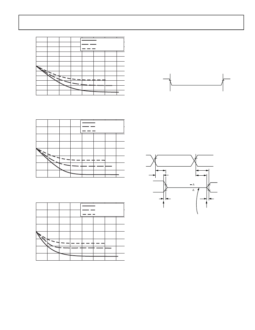
Figure 55. Driver Type E Current (3.3V V DDEXT /V DDMEM )
Output Enable Time Measurement
40
30
20
10
0
–10
–20
V DDEXT = 2.75V @ – 40 °C
V DDEXT = 2.5V @ 25 °C
V DDEXT = 2.25V @ 105 °C
V OL
Output balls are considered to be enabled when they have made
a transition from a high impedance state to the point when they
start driving.
The output enable time t ENA is the interval from the point when
a reference signal reaches a high or low voltage level to the point
when the output starts driving as shown on the right side of
REFERENCE
SIGNAL
–30
–40
t DIS
t DIS_MEASURED
t ENA
t ENA_MEASURED
0
0.5
1.0
1.5 2.0 2.5
SOURCE VOLTAGE (V)
3.0
3.5
V OH
(MEASURED)
V OH (MEASURED)
V
V OH (MEASURED)
V TRIP (HIGH)
Figure 56. Driver Type E Current (2.5V V DDEXT /V DDMEM )
V OL
V OL (MEASURED) +
V
V TRIP (LOW)
V OL (MEASURED)
(MEASURED)
20
V DDEXT = 1.9V @ – 40 °C
t DECAY
t TRIP
15
10
V DDEXT = 1.8V @ 25 °C
V DDEXT = 1.7V @ 105 °C
OUTPUT STOPS DRIVING
OUTPUT STARTS DRIVING
HIGH IMPEDANCE STATE
5
0
Figure 59. Output Enable/Disable
The time t ENA_MEASURED is the interval from when the reference
–5
–10
–15
–20
V OL
signal switches to when the output voltage reaches V TRIP (high)
or V TRIP (low). For V DDEXT /V DDMEM (nominal) = 1.8 V, V TRIP
(high) is 1.05 V, and V TRIP (low) is 0.75 V. For V DDEXT /V DDMEM
(nominal) = 2.5 V, V TRIP (high) is 1.5 V and V TRIP (low) is 1.0 V.
For V DDEXT /V DDMEM (nominal) = 3.3 V, V TRIP (high) is 1.9 V, and
V TRIP (low) is 1.4 V. Time t TRIP is the interval from when the out-
0
0.5
1.0
1.5
2.0
2.5
3.0
3.5
put starts driving to when the output reaches the V TRIP (high) or
SOURCE VOLTAGE (V)
Figure 57. Driver Type E Current (1.8V V DDEXT /V DDMEM )
Rev. D |
V TRIP (low) trip voltage.
Time t ENA is calculated as shown in the equation:
t ENA = t ENA_MEASURED – t TRIP
If multiple balls (such as the data bus) are enabled, the measure-
ment value is that of the first ball to start driving.
Page 75 of 88 | July 2013
发布紧急采购,3分钟左右您将得到回复。
相关PDF资料
ADZS-BF533-EZLITE
KIT W/BOARD EVAL FOR ADSP-BF533
ADZS-BF538F-EZLITE
BOARD EVAL FOR ADSP-BF538
ADZS-BF561-EZLITE
BOARD EVAL ADSP-BF561
ADZS-BF592-EZLITE
KIT EVAL EZ LITE ADZS-BF592
ADZS-BF609-EZBRD
KIT EVAL EZ-BOARD ADSP-BF60X
ADZS-HPUSB-ICE
TOOL EMULATOR USB HP CROSSCORE
ADZS-ICE-100B
EMULATOR BLACKFIN
AK-Y1301
CABLE SCSI-3 EXTENSION 68CONDUCT
相关代理商/技术参数
ADZS-BF527-EZLITE
制造商:Analog Devices 功能描述:ADSP-BF527 EZ-KIT Lite Evaluation Kit
ADZS-BF527-MPSKIT
功能描述:BOARD EVAL MEDIA PLAYER BF527 RoHS:是 类别:编程器,开发系统 >> 通用嵌入式开发板和套件(MCU、DSP、FPGA、CPLD等) 系列:- 标准包装:1 系列:PICDEM™ 类型:MCU 适用于相关产品:PIC10F206,PIC16F690,PIC16F819 所含物品:板,线缆,元件,CD,PICkit 编程器 产品目录页面:659 (CN2011-ZH PDF)
ADZS-BF533-EZLITE
功能描述:KIT W/BOARD EVAL FOR ADSP-BF533 RoHS:是 类别:编程器,开发系统 >> 通用嵌入式开发板和套件(MCU、DSP、FPGA、CPLD等) 系列:Blackfin® 产品培训模块:Blackfin® Processor Core Architecture Overview
Blackfin® Device Drivers
Blackfin® Optimizations for Performance and Power Consumption
Blackfin® System Services 特色产品:Blackfin? BF50x Series Processors 标准包装:1 系列:Blackfin® 类型:DSP 适用于相关产品:ADSP-BF548 所含物品:板,软件,4x4 键盘,光学拨轮,QVGA 触摸屏 LCD 和 40G 硬盘 配用:ADZS-BFBLUET-EZEXT-ND - EZ-EXTENDER DAUGHTERBOARDADZS-BFLLCD-EZEXT-ND - BOARD EXT LANDSCAP LCD INTERFACE 相关产品:ADSP-BF542BBCZ-4A-ND - IC DSP 16BIT 400MHZ 400CSBGAADSP-BF544MBBCZ-5M-ND - IC DSP 16BIT 533MHZ MDDR 400CBGAADSP-BF542MBBCZ-5M-ND - IC DSP 16BIT 533MHZ MDDR 400CBGAADSP-BF542KBCZ-6A-ND - IC DSP 16BIT 600MHZ 400CSBGAADSP-BF547MBBCZ-5M-ND - IC DSP 16BIT 533MHZ MDDR 400CBGAADSP-BF548BBCZ-5A-ND - IC DSP 16BIT 533MHZ 400CSBGAADSP-BF547BBCZ-5A-ND - IC DSP 16BIT 533MHZ 400CSBGAADSP-BF544BBCZ-5A-ND - IC DSP 16BIT 533MHZ 400CSBGAADSP-BF542BBCZ-5A-ND - IC DSP 16BIT 533MHZ 400CSBGA
ADZS-BF533-EZLITE
制造商:Analog Devices 功能描述:Microcontroller Development Tool
ADZS-BF533-MMSKIT
功能描述:KIT STARTER MULTIMEDIA BF533 RoHS:是 类别:编程器,开发系统 >> 通用嵌入式开发板和套件(MCU、DSP、FPGA、CPLD等) 系列:Blackfin® 标准包装:1 系列:PICDEM™ 类型:MCU 适用于相关产品:PIC10F206,PIC16F690,PIC16F819 所含物品:板,线缆,元件,CD,PICkit 编程器 产品目录页面:659 (CN2011-ZH PDF)
ADZS-BF537-ASKIT
功能描述:BOARD EVAL SKIT ADSP-BF537 RoHS:是 类别:编程器,开发系统 >> 通用嵌入式开发板和套件(MCU、DSP、FPGA、CPLD等) 系列:Blackfin® 产品培训模块:Blackfin® Processor Core Architecture Overview
Blackfin® Device Drivers
Blackfin® Optimizations for Performance and Power Consumption
Blackfin® System Services 特色产品:Blackfin? BF50x Series Processors 标准包装:1 系列:Blackfin® 类型:DSP 适用于相关产品:ADSP-BF548 所含物品:板,软件,4x4 键盘,光学拨轮,QVGA 触摸屏 LCD 和 40G 硬盘 配用:ADZS-BFBLUET-EZEXT-ND - EZ-EXTENDER DAUGHTERBOARDADZS-BFLLCD-EZEXT-ND - BOARD EXT LANDSCAP LCD INTERFACE 相关产品:ADSP-BF542BBCZ-4A-ND - IC DSP 16BIT 400MHZ 400CSBGAADSP-BF544MBBCZ-5M-ND - IC DSP 16BIT 533MHZ MDDR 400CBGAADSP-BF542MBBCZ-5M-ND - IC DSP 16BIT 533MHZ MDDR 400CBGAADSP-BF542KBCZ-6A-ND - IC DSP 16BIT 600MHZ 400CSBGAADSP-BF547MBBCZ-5M-ND - IC DSP 16BIT 533MHZ MDDR 400CBGAADSP-BF548BBCZ-5A-ND - IC DSP 16BIT 533MHZ 400CSBGAADSP-BF547BBCZ-5A-ND - IC DSP 16BIT 533MHZ 400CSBGAADSP-BF544BBCZ-5A-ND - IC DSP 16BIT 533MHZ 400CSBGAADSP-BF542BBCZ-5A-ND - IC DSP 16BIT 533MHZ 400CSBGA
ADZS-BF537-EZLITE
功能描述:BOARD EVAL ADSP-BF537 RoHS:是 类别:编程器,开发系统 >> 通用嵌入式开发板和套件(MCU、DSP、FPGA、CPLD等) 系列:Blackfin® 产品培训模块:Blackfin® Processor Core Architecture Overview
Blackfin® Device Drivers
Blackfin® Optimizations for Performance and Power Consumption
Blackfin® System Services 特色产品:Blackfin? BF50x Series Processors 标准包装:1 系列:Blackfin® 类型:DSP 适用于相关产品:ADSP-BF548 所含物品:板,软件,4x4 键盘,光学拨轮,QVGA 触摸屏 LCD 和 40G 硬盘 配用:ADZS-BFBLUET-EZEXT-ND - EZ-EXTENDER DAUGHTERBOARDADZS-BFLLCD-EZEXT-ND - BOARD EXT LANDSCAP LCD INTERFACE 相关产品:ADSP-BF542BBCZ-4A-ND - IC DSP 16BIT 400MHZ 400CSBGAADSP-BF544MBBCZ-5M-ND - IC DSP 16BIT 533MHZ MDDR 400CBGAADSP-BF542MBBCZ-5M-ND - IC DSP 16BIT 533MHZ MDDR 400CBGAADSP-BF542KBCZ-6A-ND - IC DSP 16BIT 600MHZ 400CSBGAADSP-BF547MBBCZ-5M-ND - IC DSP 16BIT 533MHZ MDDR 400CBGAADSP-BF548BBCZ-5A-ND - IC DSP 16BIT 533MHZ 400CSBGAADSP-BF547BBCZ-5A-ND - IC DSP 16BIT 533MHZ 400CSBGAADSP-BF544BBCZ-5A-ND - IC DSP 16BIT 533MHZ 400CSBGAADSP-BF542BBCZ-5A-ND - IC DSP 16BIT 533MHZ 400CSBGA
ADZS-BF537-STAMP
功能描述:SYSTEM DEV FOR ADSP-BF537 RoHS:是 类别:编程器,开发系统 >> 通用嵌入式开发板和套件(MCU、DSP、FPGA、CPLD等) 系列:Blackfin® 产品培训模块:Blackfin® Processor Core Architecture Overview
Blackfin® Device Drivers
Blackfin® Optimizations for Performance and Power Consumption
Blackfin® System Services 特色产品:Blackfin? BF50x Series Processors 标准包装:1 系列:Blackfin® 类型:DSP 适用于相关产品:ADSP-BF548 所含物品:板,软件,4x4 键盘,光学拨轮,QVGA 触摸屏 LCD 和 40G 硬盘 配用:ADZS-BFBLUET-EZEXT-ND - EZ-EXTENDER DAUGHTERBOARDADZS-BFLLCD-EZEXT-ND - BOARD EXT LANDSCAP LCD INTERFACE 相关产品:ADSP-BF542BBCZ-4A-ND - IC DSP 16BIT 400MHZ 400CSBGAADSP-BF544MBBCZ-5M-ND - IC DSP 16BIT 533MHZ MDDR 400CBGAADSP-BF542MBBCZ-5M-ND - IC DSP 16BIT 533MHZ MDDR 400CBGAADSP-BF542KBCZ-6A-ND - IC DSP 16BIT 600MHZ 400CSBGAADSP-BF547MBBCZ-5M-ND - IC DSP 16BIT 533MHZ MDDR 400CBGAADSP-BF548BBCZ-5A-ND - IC DSP 16BIT 533MHZ 400CSBGAADSP-BF547BBCZ-5A-ND - IC DSP 16BIT 533MHZ 400CSBGAADSP-BF544BBCZ-5A-ND - IC DSP 16BIT 533MHZ 400CSBGAADSP-BF542BBCZ-5A-ND - IC DSP 16BIT 533MHZ 400CSBGA
